Design Hardware With The imp005
Required Components, Board Layout Recommendations And Best Practices
The imp005 module was designed for customers who need enhanced networking capabilities. Not only does the imp005 support 2.4GHz WiFi (802.11b/g/n) like other Electric Imp modules, but it also supports 5GHz WiFi (802.11a/n) and wired Ethernet (10/100Mbps) connectivity.
Contents
- Important Design Notes
- Required Components
- Device Configuration Page
- PCB Layout Guidelines
- PCB Requirements
- RF Trace Routing
- Notes on the Treatment of Ethernet and WiFi Interfaces
- impOS Features Not Yet Implemented on the imp005
- LED Error Codes
- impOS Image Download
- Further Reading
Important Design Notes
GPIO and Standard Peripheral Bus Support
See Imp Pin Mux
Default Pin States
Unlike the imp001, imp002 and imp003, the imp005 does not tristate (float) all of its IO pins at start-up. Instead, the pins are set the following defaults:
| imp005 Pins | Default State |
|---|---|
| C, H, L, M, N, P, R, T, W, Y, XA | Tristate (floating) |
| B, D, K | Driven high (logic 1) |
| A, E, F, G, J, Q, S, U, V | Driven low (logic 0) |
| XB, XC, XD, XE | Pulled-up (not driven up) |
Warning: UART1_RX, UART2_RX
As you can see in the breakout board design, UART1_RX and UART2_RX both have a 1kΩ series resistor in line with the signals. The Cypress chip inside the module drives these lines as low outputs during reset, which would drive against external circuitry, so the resistors limit the current that can flow in this state.
As soon as impOS™ boots, these pins are reconfigured as inputs.
Warning: spi0, spiBCAD
The SPI peripheral in the imp005 is not as fully featured as the ones in other imps. As such, it only supports SPI_MODE_0: it cannot idle SCLK high and cannot latch data on the second edge of SCLK.
In addition, the COPI (Controller Out, Peripheral In; formerly MOSI) line holds for only ~6.25ns after the rising edge of the last bit in any transaction. Most SPI peripheral devices have a 0ns hold time requirement, so this is not problematic, but if you need to use a device which requires a longer hold time, we suggest using an R-C circuit to delay the COPI signal and extend the hold time from the point of view of the SPI peripheral.
For example, putting 47Ω resistor in series and a 1nF capacitor to ground on the SPI peripheral side of COPI will extend the hold time from ~6.25ns to around 53ns. This should be sufficient for most devices. Bear in mind that this affects both edges of the COPI signal and so you need to check that you are then not violating setup time constraints for your device. This will affect the maximum SCLK rate you can select.
If you have questions on this, please contact Electric Imp Customer Support.
Warning: i2cJK, i2c0
These buses do not support clock-stretching, so any I²C peripheral device which must delay before replying to communications from the host will not work with the imp005.
Ethernet
imp005 supports external RMII PHYs to provide 10/100Mbit Ethernet connectivity. We recommend the Microchip LAN8720A, and this is the part we have tested, but other RMII PHYs should work. Note that routing of the clocks and TX/RX pairs is critical as these signals run at high speed.
If an Ethernet PHY is not part of your design, this is automatically detected and Ethernet connections will not be attempted. If a WiFi antenna is not part of your design, no WiFi connection attempts will be made. This ensures that WiFi-only products no longer check for an Ethernet connection, and Ethernet-only products do not cause unwanted radio emissions and will save power by shutting down the WiFi sub-system.
Ethernet-only connectivity requires specific NVRAM settings to be applied: WiFi is disabled by passing the string "unavailable" into imp.setnvramimage(). This will make the following methods unavailable:
- imp.getbssid()*
- imp.getchannel()*
- imp.getcountry()
- imp.getmacaddress()*
- imp.getpowersave()
- imp.scanwifinetworks()
- imp.getssid()*
- imp.getrssi()*
- imp.rssi()*
- imp.setcountry()
- imp.setpowersave()
- imp.setwificonfiguration()
Calling these methods on a suitable configured imp005 will result in the error "index does not exist" being thrown.
Note Methods marked * have now been deprecated — imp.net.info() is now the recommended means to retrieve networking information and is not affected by disabling WiFi.
If this command is sent accidentally, the imp can be recovered by connecting via Ethernet, and running factory firmware that calls imp.setnvramimage() and passes in a valid WiFi controller settings page NVRAM image.
If this command is sent to a device with no Ethernet PHY fitted, the imp will retry after a failed connection attempt, this time using the default WiFi controller settings page NVRAM image.
USB Host
imp005 provides a USB host controller internally, and this can be connected to USB 2.0 LS/FS devices (1.5/12Mbit). The traces should be routed as 90Ω differential, as with any USB.
Due to the way USB is implemented in the imp005’s on-board Broadcom MCU, an imp005 USB connection will not operate unless pinR (USB active high load control) and pinW (active low USB fault indication) are both high.
In most applications, pinR will be used as an active-high USB load switch and hence will be high when USB is in use, but if it is not you should leave this pin unconnected but still drive it high as GPIO with hardware.pinR.configure(DIGITAL_OUT, 1).
In the case of using a load switch with an open drain nFAULT output, pinW would have an external pull-up, but if this is not present the pin should be left unconnected and configured with hardware.pinW.configure(DIGITAL_IN_PULLUP) before USB is initialized.
Currently, impOS’ USB support is limited to a single USB device connected to the imp005 at any one time. The imp005 does not therefore support the use of USB hubs.
impOS supports both Low-Speed (1.5Mb/s) and Full-Speed USB 2.0 (12Mb/s) operation.
The imp005’s USB sub-system supports Interrupt In endpoints, which provide a means for a connected device to signal the host that it needs attention. This allows customers to build more sophisticated USB support into their imp005-based applications. The imp005 can be set to poll the interrupt endpoint periodically at a rate set by a new parameter that can be passed into the existing imp API method hardware.usb.openendpoint().
See hardware.usb()
RESET_L And PWR_DWN_L
The RESET_L pin does not behave as you may expect reset to on an MCU. Though it resets some of the chip, it does not reset all subsystems to a power-on state, so we do not recommend you use this signal if you need an external reset.
When asserted, PWR_DWN_L forces a reset of the internal PMU, which produces a behavior much more like an MCU’s reset pin. Hence, we recommend that this signal is used to externally reset the device if required.
Required Components: All Designs
Your design will require the following in addition to the imp005 module.
1. BlinkUp Reception Circuitry
Please refer to the imp005 breakout board schematics, specifically the section ‘Free Run Digital BlinkUp’. This circuit is a cost-optimized circuit to implement a ramp ADC as the imp005 silicon does not have any on-board ADCs.

BlinkUp ramp ADC circuit
BlinkUp sensitivity tuning is performed by adjusting the 2200pF capacitor (C7) in much the same way as the bias resistor adjusts tuning on other imps, though smaller values of capacitor make the system more sensitive and higher values make the system less sensitive — the opposite of the bias resistor. You should use a C0G type capacitor with a tolerance of 5% or tighter to reduce device to device variation.
If low power operation is not important, you can omit Q1, C9 and R9.
2. Bi-color (Red/Green) LED to allow the imp to show users its WiFi status
This LED uses different color patterns to show different status conditions (see the BlinkUp codes guide for more information).
Your LED configuration needs to be able to produce three colors: red, green and amber. Most designs use a single bi-color LED to achieve this; some use two discrete LEDs and a lightpipe.
You may use either a common-cathode or a common-anode LED in your design; the imp005 will detect the LED polarity automatically. Two-pin (“either-or”) bicolor LEDs are not supported: it must be possible to turn red and green on at the same time. It's recommended to use LEDs with good color mixing so that red+green looks like amber. In the snippet below you can see the imp005-breakout uses a tricolor LED because these tend to have good color mixing in small packages.
A 10kΩ resistor is required in parallel with the red side of the bicolor LED to allow the imp to detect LED polarity (common cathode or common anode).

Bicolor LED circuit
3. 32Mbit or larger SPI flash
An external SPI flash part is mandatory. The minimum size of the SPI Flash is 32Mbit (4MB), and the maximum size is 128Mbit (16MB). The area below address 0x35E000 (3448KB) is reserved for use by the OS. The remainder of the available space — 648KB — is made available to user code programmatically through the Spiflash class. Areas below address 0x35E000 will be erased and reprogrammed by the OS; applications using pre-programmed SPI flash components must not use space below this address. See the imp005 datasheet for a list of recommended parts. The chosen SPI flash must support 4KB and 64KB erases across the whole of the reserved area.

QSPI boot device
Generally, a QSPI part will be used to improve boot performance; a page within the flash contains timing parameters which are used to determine the maximum clock rate and width for each part in a design. See the section on the device configuration page below.
To reduce noise in the system, source termination resistors are recommended (22R near the source of the signal, which means near the imp005 for SCLK and MOSI, and near the QSPI flash for the D1/D2/D3). Note that when running at higher speeds, trying to keep both clock and data paths clean and length matched is important.
You may download an impOS image to load into imp005 SPI flash here. This image contains the device configuration page that is described in the following sections.
4.32kHz crystal
Currently, a 32kHz crystal is a requirement for all imp005 designs.

32kHz crystal circuit
5. UART1 breakout
Designs should allow for modification so that UART1 TXD/RXD can be disconnected from application circuitry and connected to an external USB-serial cable; if a design requires RF testing (for example, it's to be used with an antenna different from the pre-approved one, or it need certification in another territory) then the WiFi part of the chip has to be driven from a PC running Cypress test code.
In this situation, you will need to build RF test units with generic Murata 1GC modules (no imp keys), preload an RF test image into SPI which electric imp can provide to you, and connect the device to a PC using a USB-serial cable. This configuration can then be made to generate the various wireless test patterns required for RF approvals tests.
Device Configuration Page
The 3448KB of SPI flash reserved by impOS includes space for a device configuration page; this information must be loaded into the SPI flash alongside the OS during production of devices based on imp005. Squirrel does not have write access to the User Info page, but Squirrel code may be used to read any data stored there. The imp API method spiflash.info() presents the data as a Squirrel table.
The User Info page is at offset 0x35d000 in the flash image.
Configuration Page Format
Information is stored in the User Info page as a variable-length data structure. The format of each entry in the User Info page is:
| Name | Type | Description |
|---|---|---|
| tag | uint16 | The type of setting |
| length | uint16 | The length of the data in bytes, not including the header. Must be a multiple of four |
| data | The settings data: one storedFlashCapabilities structure (see below) per SPI flash chip type |
At this time, the only valid value of tag is 1, for ‘flash timings’. In the future, the User Info page may be updated to provide other customer-writeable settings.
The ‘flash timings’ structure’s data field can contain a number of storedFlashCapabilities structures: one for each of the possible SPI flash chip types the customer may choose to connect to the imp005. For example, development devices may use one SPI flash chip type, production devices another. Special timings for both types can be included in the same User Info page entry, allowing the customer to cater for both device types during the production of their imp005 modules.
The length value will be 16 times the number of chip types included, ie. 32 for two types, 48 for three types, and so on. The data structure for each type, presented below, fits into 16 bytes and includes the ID (device_id) used to match against a connected chip’s JEDEC ID (see spiflash.chipid()) at boot.
struct storedFlashCapabilities {
    uint32_t device_id;
    struct {
        uint32_t size;
        uint16_t maxWriteSize;
        uint8_t fast_read_divider;    // Maximum 31
        uint8_t normal_read_divider;  // Maximum 31
        unsigned int supports_fast_read:1;  // 1 (true) or 0 (false)
        unsigned int supports_quad_read:1;  // 1 (true) or 0 (false)
        unsigned int fast_dummy_cycles:4;
    } capabilities;
};
At start up, impOS will automatically retrieve the connected SPI flash chip’s JEDEC ID using command 0x9F, storing the first byte fetched in bits 16-23, the second byte in bits 8-15 and the third byte in bits 0-7. It will then scan the User Info page for an entry of tag equal to 1. If such an entry is found, impOS reads each of the storedFlashCapabilities structures stored in the entry’s data field and attempts to match the SPI flash chip’s JEDEC ID with a device_id value. If there is a match, impOS uses the contents of that device_id’s associated capabilities record to program the SPI flash chip’s timings.
This allows the customer to program special timings which will be used from this point on. Up until this point — or if no special timings are found — impOS connects to the SPI flash chip using default timings, which are single-bit-wide SPI at ~5.3MHz.
The internal bus clock is 160MHz, so the fast_read_divider and normal_read_divider reference this source clock; also note that the LSB of the divisor is ignored, so the effective range is 2 (80MHz) to 30 (5.33MHz). In our experience, a design with a good layout is safe running with a divisor of 6, resulting in a clock rate of 26.66MHz.
The recommended settings are:
- Quad read enabled
- Fast read disabled
- maxWriteSize is one page (256 bytes)
A dump of a config page might look like this:
0000000 01 00 50 00 17 20 c2 00 00 00 80 00 00 01 06 06
0000010 22 00 00 00 17 40 01 00 00 00 80 00 00 01 06 06
0000020 22 00 00 00 17 bb 20 00 00 00 80 00 00 01 06 06
0000030 22 00 00 00 17 ba 20 00 00 00 80 00 00 01 06 06
0000040 22 00 00 00 17 40 ef 00 00 00 80 00 00 01 06 06
0000050 22 00 00 00
- 01 00 : tag 0x0001 (flash capabilities)
- 50 00 : length 0x0050 (5 entries of 16 bytes each)
- Flash 1: 0x1720c200, JEDEC code 0xc2, 0x20, 0x17 (Macronix MX25L6433F)
- Flash 1: 0x00008000, Size of 0x00800000 (8MB, 64Mbit)
- Flash 1: 0x0001, Max write size of 0x0100 (256 bytes)
- Flash 1: 0x0606, Fast read and quad read divisor of 6 (26.66MHz)
- Flash 1: 0x00000022, 2 dummy cycles (not used) and quad read enabled
As you can see, there are four other devices with identical settings in the config page. These are JEDEC 0x014017 (Cypress S25FL164K), JEDEC 0x20bb17 (Micron N25Q064A13ESE4), JEDEC 0x20ba17 (Micron N25Q064A13ESED; improved erase speed vs ESE4), JEDEC 0xef4017 (Winbond W25Q64FV).
PCB Layout Guidelines
It’s very important that your design follow a few simple rules when it comes time to place and route your printed circuit board in order to take advantage of the imp005’s simplicity and maximize performance.
1. Minimize impedance to ground
The imp005’s ground pins should have a clear path back to ground, without running through many narrow traces or bottlenecking at a single via. While a via may be rated for much more DC current than your design calls for, the impedance of the ground path needs to be as low as possible to prevent noise from becoming a problem in your design. This applies to other parts of your design as well, so minimize ground impedance everywhere.
Use Ground Pours Flood ground on the top and bottom of your PCB to provide a good ground path to all components. The imp005’s antenna tuning ‘expects’ a ground pour under the non-antenna portion of the imp. If the ground pour is omitted, the antenna will be de-tuned, which will negatively impact range and performance, and may prevent your product from passing wireless certifications.
Stitch ground planes around the edge of your board and throughout the interior of the board. Use more vias than you need for the DC current your circuit requires; this will lower the impedance of the ground paths and reduce noise.
2. Place bypass and filter capacitors as close to VDD pins as possible
Bypass capacitors will dump noise to ground, but if the trace on the filtered side is long, it presents an opportunity for that trace to pick up noise again.
3. Do not tie VDD pins together directly
Use "V" routes to connect power pins to power planes even if they are adjacent to each other; this applies to pins A56 and A57 specifically — the route adds some inductance and hence noise isolation.

V routing to adjacent power pins
4. Route between VDD_3V0_OUT and VDD_3V0_IN is critical
This trace is very noise critical. It is strongly recommended to route this on layer 3 (power plane), sandwiched between an unbroken ground on layer 2 (ground plane) and layer 4.

Power plane island connecting VDD_3V0 IN and OUT pins on imp005 breakout
5. Pull back ground around 32kHz crystal on top layer and layer 2
The parasitic capacitance of a nearby ground plane may exceed the required load capacitance for your 32kHz crystal (if used). To avoid de-tuning the crystal (which can severely affect performance or prevent the imp005 from operating entirely), pull ground pours back around the 32kHz crystal and crystal load capacitors.

Ground Pour pulled back around 32kHz crystal
6. Always follow the recommended layout in the manufacturer datasheet for any switching power supply
A poorly-routed switching power supply will send noise all over the board and severely impact performance and range. This is easily avoided by following the recommended layout in the datasheet for nearly any switching power supply IC.

Recommended Layout for the TPS62172 Buck Regulator, as shown in TI’s datasheet
Noise on your board directly diminishes your WiFi performance, and can prevent you from passing FCC certifications. Keep all noisy parts (switching power supplies, high-speed signalling) as far from the imp’s antenna as possible.
7. Prioritize your signal routings
Routing signals in the correct order can significantly simplify a design:
Place your power supply and route VDD It’s generally a good idea to avoid vias on your power supply rail; these increase the impedance of the trace and create an opportunity for noise to impact your design.
Route high-speed signals directly and avoid vias By keeping the path between devices that communicate over a high-speed interface such as SPI direct and short, you minimize the possibility that noise will couple into the line, or that the signals on the line will couple into other parts of your design as noise.
Keep analog signals clear of noisy digital signals, and route them as directly as you can Routing an analog signal right next to a digital signal creates an opportunity for digital noise to couple into the analog signal. Keep them apart and pour ground in between to provide some shielding.
Route GPIOs last A signal which is simply used to poll a button or toggle an LED does not need special considerations. If a GPIO signal crosses a higher-priority signal such as a SPI bus or an analog line, the lower-priority signal should via around the higher-priority one.
PCB Requirements
Because a board incorporating the imp005 must include a microstrip transmission line from the imp005 to the antenna, a four-layer PCB is required in order to achieve 50Ω impedance control of the RF trace.
RF Trace Routing
Murata has performed CE pre-testing and FCC/IC modular certification for the type 1GC module (imp005) with their own dual-band PCB antenna design. Designs derived from these reference designs, using the same layer stackup and antenna design, and carefully adhering to the relevant layout guidelines here, may attach and re-use the relevant modular certification rather than repeating FCC/IC intentional emitter testing.
Note that modular certification is only available for the 1.6mm board thickness.
Layer Stackup
Modular pre-certification has been performed with the layer stackup shown below. If a different layer stackup is used, modular certification may not be used. Note that changing the layer stackup will also affect the values of the RF matching components and possibly the dimensions of the RF trace in order to maintain a 50Ω characteristic impedance.

Layer Stack used for imp005 pre-certified design
RF Trace
The RF trace must be a 50Ω ± 2Ω impedance controlled transmission line which is referenced to a solid, unbroken ground. The trace width and distance to the ground plane must be adjusted to achieve the target impedance. The trace should not have sharp changes in direction and should use curved traces when needed. You will need to tell your PCB vendor which trace requires impedance control and ask for per-lot testing & reports to ensure that they are meeting the requirements.
The RF_OUT pad on the imp005 is surrounded by ground pads; these should be tied together to form a a ground reference around the end of the RF trace. The RF trace should be kept as short as possible. Sharp bends should be avoided in the RF trace.

Detail view of the RF_OUT pad on the imp005 design
PCB Antenna
The antenna must be placed at the edge/corner of the PCB, with a copper keep-out under the entire antenna element on all PCB layers. No other traces or components may be placed in this region. A row of stitching vias is required along the edge of the ground pour below the antenna section; this ground pour, including the vias, is part of the antenna. The module, antenna, and RF trace must all be placed on the top layer of the board.
The antenna may be mirrored (left/right) as required for mechanical design as long as the dimensions of the antenna are preserved and all other design rules are followed. Please consult the gerber files for imp005-breakout to obtain the exact measurements, and the BOM for the exact component part numbers that are used within the antenna pattern. You should not substitute any other parts; the capacitor must be a Murata GJM1555C1H1R0BB01D and the inductor must be a Murata LQG15HS3N0S02D.
If the antenna is on the corner of the board, ensure that there is >=16mm between the antenna edge and the nearest groundplane (or board edge) horizontally.
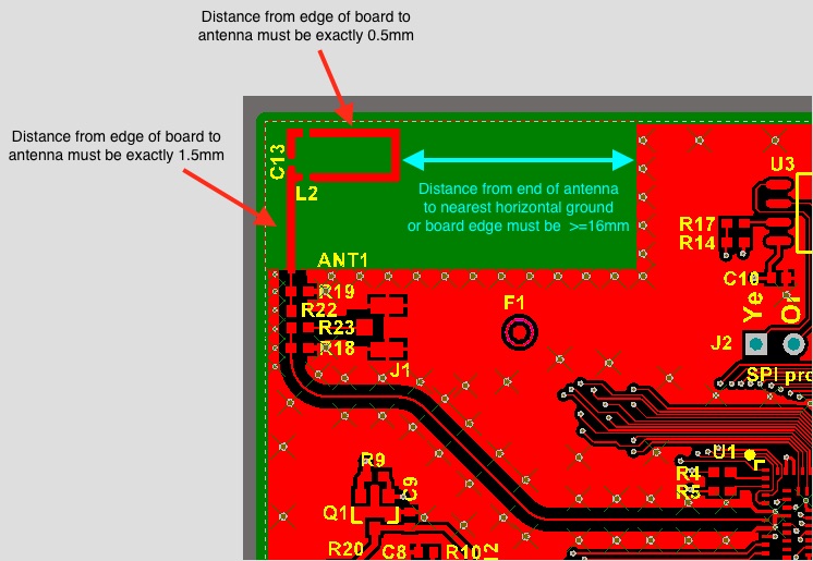
Antenna detail
Notes On The Treatment Of Ethernet And WiFi Interfaces
Initial Connection
Before an imp-enabled device can be used, it must be authorized to access the Electric Imp impCloud™. This process is called ‘enrollment’ and it takes place when the device is first configured for Internet access. Configuration is typically performed using Electric Imp’s BlinkUp technology. No imp-based device is permitted to connect to an impCloud until it has been enrolled.
Until an imp005-based device has been configured using BlinkUp, it cannot connect to a wireless network because it has no stored WiFi network access credentials — a local network’s SSID and its security password. Although the imp005 needs no credentials to connect via an Ethernet network, it will not connect at this time even if joined to an active wired link.
If the imp005-based device is connected to an active Ethernet network when BlinkUp takes place, the subsequent connection to the enrollment server will take place via the wired link. Any WiFi credentials passed during BlinkUp will be stored but, for now, ignored.
Ethernet-only devices should disable WiFi passing the string "unavailable" into imp.setnvramimage(). This ensures Ethernet-only products do not cause unwanted radio emissions and will save power by shutting down the WiFi sub-system. It also disables WiFi-centric imp API methods. See the ‘Ethernet’ section, above, for more information.
Subsequent Connections
When an enrolled imp005-based device starts up, either from a warm or a cold boot, it will first attempt to connect over Ethernet. If no link is detected, it will attempt to connect using the WiFi networking information supplied during BlinkUp, if any. If this attempt also fails (there may be no local wireless network, or the imp may have no valid WiFi network information on board), then the imp005 will once more try to connect using Ethernet. It will continue to cycle between Ethernet and WiFi until it makes a successful connection with one of them. If no connection is initiated within ten seconds of start-up, impOS will begin running application Squirrel. The attempt to connect by one means or another will continue in the background.
Devices with no Ethernet PHY will not attempt to connect by Ethernet and will instead immediately try to connect by WiFi. The imp.getethernetspeed() API will not be present in this case. See the ‘Ethernet’ section, above, for more information.
However the device eventually connects, this will become its current ‘preferred’ connection method. For example, if the device successfully connects using WiFi and then experiences an unexpected disconnection, it will typically attempt to reconnect using WiFi, whether there is an active Ethernet link or not.
However, if a reconnection attempt using one network type fails, the device will attempt to use the other type — assuming the other type has not been disabled.
If the imp is disconnected manually, using the server.disconnect() imp API method, then even if the imp’s disconnection policy is set to RETURN_ON_ERROR, when server.connect() is eventually called, it will nonetheless attempt to connect first via Ethernet and, if that fails, by WiFi. This is intentional: it provides application programmers with a means to manually switch network modes, for example if is the device is connected to an Ethernet network after start-up and subsequent to the device connecting to a WiFi network. Again, this behavior is modified if either of WiFi or Ethernet is disabled.
Manual Reconnection
Squirrel code can call the imp API method imp.net.info() at any time to determine whether the device is currently linked to an Ethernet network, even if the imp is not communicating with the server over that link. If the integer returned by this method is non-zero (it will be 10 or 100, representing the rated link speed), the application can explicitly disconnect from the current network (presumably WiFi) and immediately attempt to reconnect to the server.
As outlined in the section above, this will use the newly connected Ethernet link. It therefore provides a means for code to periodically check whether an end-user has hooked the device up to an Ethernet network subsequent to its initial connection to WiFi.
Of course, if the imp is already connected using Ethernet, this switch is unnecessary and so the device code should, for example, check imp.net.info() at start-up to determine whether it is connected by Ethernet or WiFi, and only if it is using the latter does it need to poll for the ad hoc connection of an Ethernet cable.
impOS Features Not Yet Implemented Or Partially Implemented On The imp005
The following standard impOS features are not yet enabled on the imp005:
- Deep sleep modes imp.deepsleepfor(), imp.deepsleepuntil(), server.sleepfor() and server.sleepuntil()
- Wireless configuration using WiFi Protected Setup (WPS)
- Device-side persistent storage via the nv table
- Real-Time Clock operation
LED Error Codes
Because the imp005 loads WiFi configuration and operating system data from external flash storage, it must check that the flash is connected and can be read. This takes place at start-up, and any errors encountered are signalled on the three-color LED attached to the imp005. The following table lists these error signals; click on an error’s Play link to view an animation of the LED pattern.
Note that if the flash is blank, or is corrupt, the cryptographic check on the image will fail and the device will be unable to show any failure LED code because no impOS is able to be loaded. In this case, you will see the green LED lit solidly at a low brightness level if you have a common cathode LED, or no LED indication at all if you have a common anode LED.
| SPI Flash not found | 500ms | 250ms | Repeat | |||||||
|---|---|---|---|---|---|---|---|---|---|---|
| SPI Flash error | 500ms | 250ms | Repeat | |||||||
impOS Image Download
Get the latest impOS firmware for pre-installation on device SPI flash.
Further Reading
- imp API: spiflash.size()
- imp API: spi.chipselect()
- imp API: spi.configure()
- imp API: imp.setnvramimage()
Document History
| Date | Notes |
|---|---|
| November 24, 2021 | Add link to impOS downloads page |
| February 04, 2019 | Add impOS 38.17 download |
| October 30, 2018 | Minor corrections |
| August 03, 2018 | Correct imp005 datasheet links |
| July 03, 2018 | Add impOS 36.10 download |
| March 22, 2016 | Added preliminary impOS 36-related changes to Ethernet and USB sections |
| October 14, 2016 | Added impOS 34.9 download link; updated ‘LED Error Codes’; added spi0, spiBCAD note |
| October 13, 2016 | Added ‘LED Error Codes’ |