SPI Explained
An Introduction To The Standard Serial Peripherals Bus
The Serial Peripheral Interface (SPI) was developed by Motorola to allow its chips to communicate with each other, much as Philips devised the I²C serial bus for its own integrated circuits. While these two buses do largely the same job, both have become almost equally commonplace, and many peripheral devices use either one or the other to communicate with a host microcontroller. This ubiquity is why imps support both of them.
SPI has some advantages over I²C, in particular support for higher data transfer rate. SPI also has a duplex capability which makes it particularly suitable for those applications that require simultaneous two-way communication.
On the other hand, SPI requires at least three wires, shared by all the devices on the bus, and a number of device-selection lines, one for each peripheral connected to the controller device. I²C, by contrast, requires only two wires; it uses unique addresses to identify all the devices on the bus. This makes working with multiple devices more straightforward than SPI’s address-less approach, though some developers prefer using hardware to select a device rather than address data.
Controllers And Peripherals
SPI separates devices into ‘controllers’ and ‘peripherals’. Only one device can send out timing pulses to synchronize data transfers, and that’s the one chosen to be the controller. All others, which synchronize their timings with the controller, are considered subsidiary peripherals. The controller — which in your product must currently be its imp — and its peripherals can all transmit and receive data, but only the controller can establish the timing pattern to which they all operate. This establishment of a fixed timing scheme is what makes SPI, like I²C, a ‘synchronous’ bus.
The Physical Bus
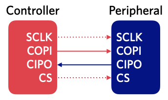
The imp’s SPI implementation has four lines:
- SCLK, the serial clock signal from the controller.
- COPI, short for ‘Controller Out, Peripheral In’ (sometimes labelled MOSI in old datasheets).
- CIPO, short for ‘Controller In, Peripheral Out’ (sometimes labelled MISO).
- CS, short for ‘Chip Select’ (sometimes labelled SS, nSS or SYNC)
COPI and CIPO are the data-transfer lines.
The imp001 and imp002 don’t provide dedicated CS pins: instead you can use any of these imp’s other GPIO pins. The imp003 and up provide dedicated CS pins as part of their SPI buses, marked on the imp pin mux page.
Note The imp005 provides a dedicated chip select pin on each of its two SPI buses. For spiBCAD this is pin D; for spi0 this is pin CS0. The imp API method chipselect() can be used to take control of the assertion and de-assertion of these chip select pins (please see the method documentation for more information).

SPI on the imp: up to four lines connect to a single peripheral device
This approach follows Motorola’s definition of SPI: that each bus transaction — essentially a batch of data bytes — should be linked to a specific peripheral. Texas Instruments modified the SPI specification to allow each byte to be send to a specific peripheral, though this requires a dedicated CS line. This mode is not currently supported by any imp.
Signalling
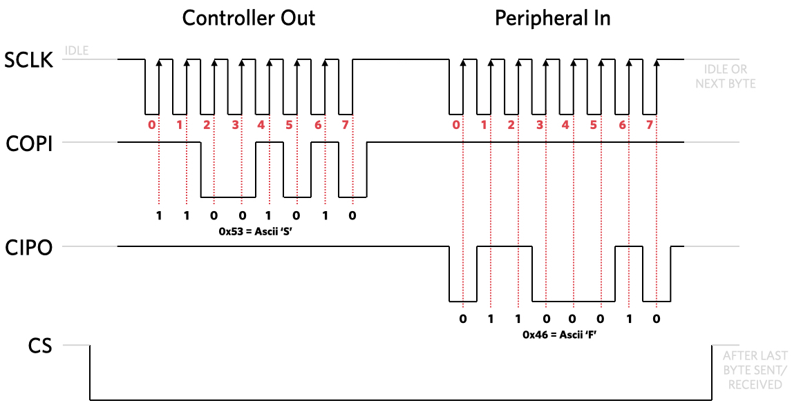
Assuming we have a single peripheral connected to the controller, communications are initiated by the controller pulling the CS line low. The tells the peripheral to get ready to converse. Now the controller begins sending clock pulses out along the SCLK line; typically data transmissions are keyed to the rising edge of each pulse, though that’s not always the case.

Clocking the data in and out: the imp sends a command, the peripheral returns data
The controller will now transmit data on the COPI line, actively driving the line high to signal a 1 or low for a 0. The peripheral will read the signal — which might be a command for a sensor reading to be sent, for example — and it will return that information on the CIPO line, again driving the line to stay high to signal a 1 or driving it low to transmit a 0. This requirement that the line be actively driven high or low, rather letting it settle to one state or the other by connecting a resistor, is the reason SPI can support higher speeds than I²C can. I²C loses transmission time while its pull-up resistor returns the line to high.
That said, it’s nonetheless good practice to also have a pull-up on an CS line to ensure that it goes high when the imp is booting or sleeping and therefore not able to drive the line high manually. Keeping the line high ensures the peripheral will ignore any glitches on the data and clock lines.
When the controller has what it wants, it drives the CS line high once more, and the peripheral can rest.
imp SPI Options
Every imp has a number of independent SPI buses, accessed as properties of the device’s hardware object, which is instantiated at start-up. Each imp’s pin mux table shows that there are many choices, depending on which type of imp you are using in your product. This document assumes you are using an imp001, so you should consult the pin mux table if you are working with a different imp. The imp001’s two SPI buses are both three-wire implementations of the bus, and connected to pins 1, 8 and 9, and 2, 5 and 7, respectively. Pins 1 and 5 are SCLK; 8 and 7 COPI; and 9 and 2 CIPO. Whichever of the two buses you use, it’s good practice to alias it at the outset:
spi1 <- hardware.spi257;
spi2 <- hardware.spi189;
Configuring either for use is simply a matter of telling the imp how fast you want the bus to run, and to provide a set of constants which together determine how the bus will operate:
spi1.configure(modeFlags, speed);
First, the speed. This is simply an integer value giving the throughput in kiloHertz (kHz):
The specific SPI data rates available (in kHz) are as follows:
| imp001, imp002 | imp003 | imp004m | imp005 | imp006 | |
| spi189 | spi257 | spiEBCA spiLGDK | spiAHSR spiGJKL | spiBCAD spi0 | spiXTUVW |
| 15,000 | 30,000 | 18,000 | 24,000 |
The SPI data rates available range from 5KHz to 22.8MHz The SPI is clocked by dividing 160MHz by any integer from 7 to 32,000 inclusive |
Min. 187KHz, max. 750KHz |
| 7500 | 15,000 | 9000 | 12,000 | ||
| 3750 | 7500 | 4500 | 6000 | ||
| 1875 | 3750 | 2250 | 3000 | All others | |
| 937.50 | 1875 | 1125 | 1500 | Min. 187KHz, theoretical max. 24MHz | |
| 468.75 | 937.50 | 562.50 | 750 | ||
| 234.375 | 468.75 | 281.25 | 375 | ||
| 117.1875 | 234.375 | 140.625 | 187 | ||
An imp will automatically select the closest speed to that value that the peripheral supports, and it returns this final speed value:
local actualSpeed = spi1.configure(CLOCK_IDLE_LOW, preferredSpeed);
The mode flag(s) can be selected from the following list of constants:
| Constant | Meaning |
|---|---|
| SIMPLEX_TX | One wire (plus clock) transmitter only |
| SIMPLEX_RX | One wire (plus clock) receiver only |
| CLOCK_IDLE_HIGH | Clock idles high |
| CLOCK_IDLE_LOW | Clock idles low (default) |
| CLOCK_2ND_EDGE | Clock the second (trailing) edge |
| MSB_FIRST | Send most significant bit first (default) |
| LSB_FIRST | Send the least significant bit first |
| NO_SCLK | SCLK pin is not used |
| USE_CS_L | Enable the use of the dedicated chip select pin (imp005 only) |
These can be combined, if you need them to be, using the logical OR operator, |, though some are mutually exclusive so should not be combined: SIMPLEX_TX and SIMPLEX_RX, for example. To use both CLOCK_IDLE_LOW and CLOCK_2ND_EDGE, for instance, instead of entering a single constant as a parameter in the configure() method you would include both, separated by the | symbol:
spi1.configure(SIMPLEX_TX | MSB_FIRST | CLOCK_IDLE_LOW, 400);
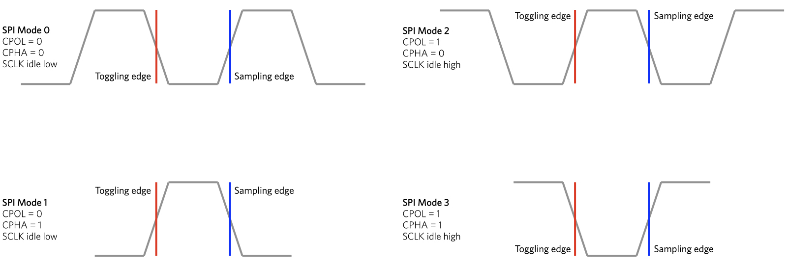
Combinations may be necessary if they are specified by the peripheral’s datasheet, though this may not be immediately obvious to the newcomer. Datasheets may talk about a device’s ‘SPI Mode’, or its CPOL (Clock POLarity) and CPHA (Clock PHAse) values. CPOL and CPHA determine which edges of the clock signal are used to drive and sample data signals. Each of these two parameters has two possible states, for four possible combinations in all:

SPI Modes
SPI Modes simply index those combinations rather than the separate CPOL and CPHA values. The controller and the peripheral have to communicate using the same CPOL and CPHA values, and thus the same Mode. Multiple peripherals may well mean different configurations, so the controller will have to reconfigure itself each time it needs to communicate with a specific peripheral.
You can convert from Modes and CPOL/CPHA values to imp API constants using the following table:
| Mode | CPOL | CPHA | Imp API Constant(s) |
|---|---|---|---|
| 0 | 0 | 0 | CLOCK_IDLE_LOW |
| 1 | 0 | 1 | CLOCK_IDLE_LOW | CLOCK_2ND_EDGE |
| 2 | 1 | 0 | CLOCK_IDLE_HIGH |
| 3 | 1 | 1 | CLOCK_IDLE_HIGH | CLOCK_2ND_EDGE |
Reading And Writing Data
Having configured the SPI bus, use the write() method to send a string of bytes to the peripheral device:
spi1.write("This is an LCD display");
Use of a string is optional: you can also send a blob of raw data bytes:
local blob = blob(4);           // Create a four-byte blob...
blob.writen(0xDEADBEEF, 'i');   // ...and write a 32-bit value to it
spi1.write(blob);
Whether you want to read a string or a blob, you need one of the imp API’s two SPI read methods:
local bytes = spi1.readblob(8);
local inputString = spi1.readstring(16);
The integer value passed as a parameter is, respectively, the number of bytes to be read into the blob and the number of characters to be put into the string. Of course, since one character takes up one byte, these two methods are equivalent. The latter simply converts blob to string for you.
Because of the ‘full duplex’ nature of the SPI bus, writes and reads always occur simultaneously. With the read and write commands we’ve seen so far, data moving in the opposite direction from the one we are interested in is ignored or zeroed. So, when you write a string, say, any data arriving at the imp from the peripheral is ignored. During either of the two read operations, a matching size of ‘dummy’ zero bytes is written to the peripheral: if you read eight bytes, say, eight 0s are written automatically.
To manage this simultaneous two-way communication, the imp API has a fourth method which combines reads and writes:
local inputString = spi1.writeread(outputString);
So, as the string outputString is being sent out along the COPI line, the variable inputString is being filled by the data bytes coming on on CIPO. You can send and receive strings or blobs, but both input and output must be of the same type. However large your output blob, your input blob will be of the same size. Likewise, input and output strings will be of the same length.
Full duplex operation can also be used with device that do not expect to operate that way — those that require the read and write ‘dummy’ bytes to be a specific, non-zero value. This requirement rules out using the regular write(), readblob() and readstring() methods, but writeread() can be used in their place to make sure the device’s preferred dummy values are used.
Example Code
The following code works with the Analog Devices ADXL345 digital accelerometer, a part that uses SPI to communicate with its host microcontroller. It also supports I²C, and the pins on this Adafruit breakout board, which is based on the chip, are labelled accordingly. The chip’s datasheet can be downloaded from the Analog Devices website.
How The Code Works
We use an imp001’s spi257 bus, aliased near the beginning of the listing as spi. We also alias pin 8 as the CS line. The function spiWriteReg() shows how these are used. A write transaction is signalled by switching the CS line low. Next the address of the register we want to write to is converted from a Squirrel 32-bit signed integer to an 8-bit value by writing it to a blob. This blob is then written to the SPI bus. We do the same thing with the value we want the ADXL345 to put into that register, and then we set the CS line high again to signal the end of the transaction.

The Adafruit/Analog Devices ADXL345
The function spiReadReg() works in the same way, only this time we read value data from the bus after writing the source register’s address. The ADXL345 requires some adjustments to be made to the register address in this instance: bit 7 needs to be set in order to mark the transaction as a read operation, and bit 6 needs to be set to tell the chip that we expect more than a single byte to be sent back.
Where the program proper starts, we configure the imp’s SPI bus to match the requirements of the ADXL345 chip. It uses SPI Mode 3 — ie. both CPOL and CPHA should be set — so we use the equivalent imp parameter: CLOCK_IDLE_HIGH | CLOCK_2ND_EDGE in the configure() call. We also set the speed to 100kHz. Next, the imp’s pin 8, which is operating here as the CS pin, is configured as a digital output and set high.

Wiring up the ADXL345
Other functions in the program initialize the ADXL345 itself rather than the SPI bus. The ADXL345 is initialized, and the code reads in the value from register address 0x00 to ensure the device is present on the bus. The chip has a self-test mode which allows a series of calibration readings to be taken; this we do and store the results. Later, in the function loop(), these values are used to adjust the final readings from the accelerometer.
The ADXL345 saves its x-, y- and z-axis samples as 16-bit values, each in two 8-bit registers; loop() uses the spiReadReg() function to acquire each value’s two components and then converts them into single values by multiplying the most significant byte by 256 and adding to the result the value of the least significant byte.